
The first step in the wafer grinding process is backgrinding, which begins with a large-grit wheel. After this step, the silicon wafer is polished with finer grit wheels. Deionized water is used to remove any debris from the wafer surface. The front surface of the silicon wafer is protected with a protective tape. Wafer grinding can be performed in an ultra-thin configuration, allowing for the production of extremely thin wafers.
Process
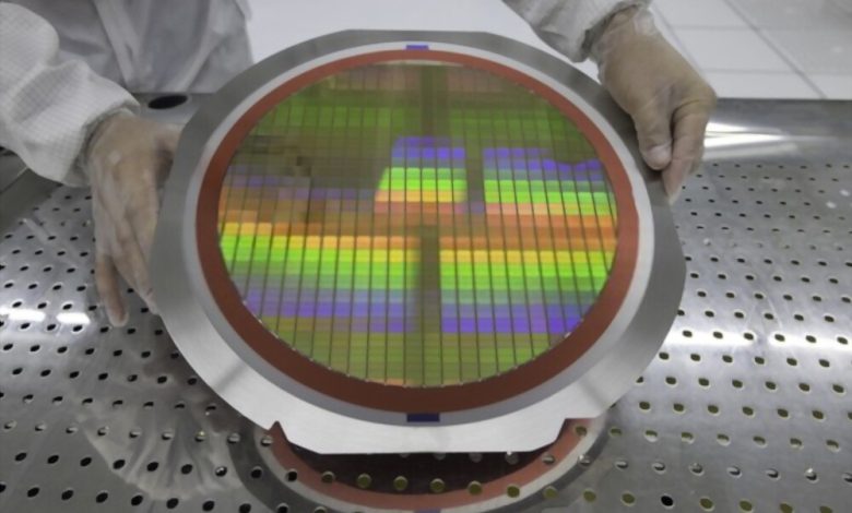
Process of wafer grinding is an important stage in semiconductor manufacturing. Often wafers with 200 mm diameter start at 720 um and are then sliced in half. Wafers are then ground on the backside to achieve the required thickness. Grinding causes a loss of yield because it exposes the front of the wafer to contaminants. A typical two-step backgrinding operation uses dual spindles with grinding wheels on each.
A grinding wheel 34 rotates on a chuck table. The abrasive member contacts the back surface W2 of the wafer. The wafer is then grinded to a predetermined thickness with the abrasive member. This results in the formation of a strain layer 10 on the back side of the wafer. A strain layer 10 is formed on the back side of the wafer, which is removed during thinning.
Two main types of abrasive members were used in this study. The first type grinds the wafer’s back side with an abrasive member B. Abrasive members A and B had similar operational conditions, but the final grain size was different. For this reason, it is important to choose the abrasive member that best meets the requirements of your project. These are the two main ways of grinding wafers.
Mechanical backgrinding is the most common method for thinning wafers. It is more efficient than plasma etching and chemical etching. However, this method can cause damage to the wafer by adding mechanical stress and heat to the wafer, as well as resulting in scratches. Wafers with thin backsides require a higher grinding step. However, it is also important to know the process of backgrinding.
Tools
When it comes to dicing and grinding silicon wafers, it helps to know which tools are required. Diamond grinding tools from Meister Abrasives are ideal for this process, with TTV values in the low one digit Angstrom range. A ceramic and hybrid bonded grinding tool, on the other hand, represents a quantum leap in reliability and quality for semiconductor applications. These tools can be used for Si, GaN, and other materials that require a high degree of spherical or cylindrical shape.
If a company is using a conventional wafer grinder, it is important to choose the proper coarse grind wheel. A coarse grinding wheel with the proper grain size can increase yields. If the coarse grind wheel is too coarse, subsurface damage can occur, which can further reduce yields. Ultimately, tools for wafer grinding are a critical component of the semiconductor fabrication process. Fortunately, there are several different choices when it comes to wafer grinding machines.
The Surface Grinding/Polishing Machine 72/860 is a machine used in manufacturing multi-crystalline and mono-crystalline silicon wafers. It can grind silicon bricks and square ingot segments to a mirror-like finish. Then, it must be chamfered or rounded over with a round grinding machine 72-856. In addition to the surface grinding process, wafers must be prepared for post processing.
The demand for semiconductor tools is high, and it is likely to continue growing throughout the forecast period. With the advent of new technologies and increasing demand for miniaturized integrated circuits, the semiconductor industry is expected to experience rapid growth in the next few years. The latest tools and machinery designed specifically for this process will continue to grow at a rapid pace. The following information on tools for wafer grinding will help you decide which machines and equipment are right for your needs.
Techniques
Several techniques exist to produce thinning layers on a silicon wafer. One technique is mechanical backgrinding, which is faster than plasma etching and chemical etching. The downside of mechanical backgrinding is the risk of mechanical stress and heat, and the process can cause scratches on the backside of the wafer. This method is generally less expensive and faster than plasma etching. Techniques for wafer grinding involve using an abrasive slurry that removes material from the wafer.
Another method of wafer grinding is back-ground grinding, which reduces the thickness of the wafer to 80-70um. It is then stacked up to 16 or 32 layers, each of which is a tenth of its original thickness. This process produces a semiconductor multi-layer structure, known as a Multi Chip Package. These semiconductors must be a minimum total height of 1.4mm. However, in many cases, the back-ground wafer is thinner than the final product, which can be a significant drawback.
Another technique that produces thinner wafers is CMP. This method produces semiconductors with near-perfect flatness and controlled TTV. Wet etching, on the other hand, uses liquid chemicals to remove material. It is useful for selective thinning of wafers, and isotropic or anisotropic thinning. However, it is not ideal for grinding wafers with defects. It is important to choose the correct grinding technique for your needs.
Wafer lapping is an excellent technique to remove surface damage on semiconductors and improve their flatness. During backside grinding, warpage becomes a primary cause of failure. In addition to Raman spectrometry, this process can be modeled numerically, incorporating various factors that can cause warpage. This can reduce the risk of warpage and increase the yield of a product. Abrasive lapping also produces wafers that are flatter and more efficient than non-bonded silicon-silicon wafers.
Want to read more: Click here: https://www.stealthdicing.com/about-gdsi/
Limitations
During the manufacturing process, wafers undergo a series of operations to remove layers and damage. The semiconductor wafer is then polished chemically and mechanically. Grinding the wafer to a certain thickness can minimize the chances of breaking the wafer. There are also some limitations to wafer thinning. Wafers with a minimum thickness can be regenerated. If the grinding process is done incorrectly, breakage can occur.
The most common process for thinning wafers is mechanical backgrinding. This method is more affordable and faster than plasma etching, but it has a few disadvantages. It can result in excessive heat, mechanical stress, and scratches on the backside of the wafer. The grit size of the grinding process also determines the pressure applied to the wafer. This process can also produce central bumps, which can cause poor site flatness.
The thickness of the wafer will be a limitation of the backside grinding process. For thin wafers, the process is more complex than with thicker ones. Wafers with higher resale value will require dicing, but this cannot be done before the grinding process. Besides, the presence of back side alignment complicates the dicing process. During dicing, the backside alignment of the wafer will affect the overall performance of the process.
When the backside grinding process is applied to wafers, it’s possible to eliminate as much as 90 percent of the excess material. The resulting silicon dross can be recycled and used again. It’s also possible to use the silicon residue as fuel. The silicon dross is a by-product of the grinding process, and this waste material is useful to the company’s bottom line. If you’re wondering about the benefits of backside grinding for wafers, read on.
New technology
The advancement of back grinding technique has been a long-term goal of many semiconductor companies. It enables them to achieve the lowest defect levels for next-generation devices. This technique combines two processes to produce perfect wafers. The first one, called rough grinding, requires rough grinding while the second, known as fine grinding, uses fine grinding. In both processes, a slurry or deionized water is inserted between the wafer and the pad.
The other method uses magnetic position control to automatically control the ID grinding wheel’s axial position, making it possible to produce ultra-thin wafers. The new technique is very efficient and can be used to produce wafers up to 150 mm in diameter. To make this process efficient, a new conditioning strategy must be developed. This method must consider factors such as process automation, tool life and wafer quality. Moreover, the new technique must be cost-efficient.
The process reduces the thickness of back-ground silicon wafers from 800 to 70um. The wafers are then stacked to an average of four to six layers, and up to 32 layers are possible. The end result is a multi-layer semiconductor structure, called a Multi Chip Package. Moreover, the total height of a Multi Chip Package must not exceed 1.4mm. These improvements are significant to the semiconductor industry and will help in the production of chips in the future.
Improved wheel performance: The next generation #8000 wheel is highly effective in improving the quality of ground wafers. The high-quality surface finish provided by the new wheels reduces bow and improves the die strength. The advanced process also reduces post-grinding operations. It also allows for increased throughput and improves wafer geometry. If you are considering upgrading the abrasive wheel in your wafer grinding facility, this technology is a great investment.
Thanks for visiting articlsoup